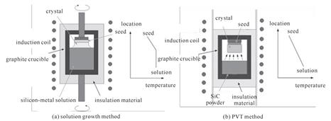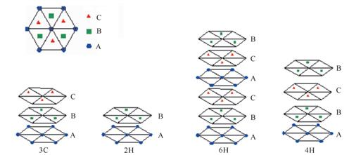
碳化硅作为第三代宽禁带半导体的核心材料之一,相对于传统的硅和砷化镓等半导体材料,具有禁带宽度大、载流子饱和迁移速度高,热导率高、临界击穿、场强高等诸多优异的性质。基于这些优良的特性,碳化硅材料是制备高温电子器件、高频大功率器件的理想材料。近年来在碳化硅材料生长和器件制备方面取得重大进展,对碳化硅材料特性和生长方法进行回顾,并研究了碳化硅光导开关偏压、触发能量、导通电流之间的关系,以及开关失效情况下电极表面的损伤情况。
As a key representative material for the third-generation wide bandgap semiconductors, silicon carbide (SiC) is a promising wide band gap semiconductor material and can be used for the fabrication of high-power and high-frequency electronics, due to its superior physical properties, such as high thermal conductivity, wide band gap and high critical breakdown field. In recent years, bulk growth of SiC single crystals and the fabrication of devices have made significant progress.
The paper introduces the growth techniques for SiC bulk and presents the relationship between the on-state resistance and voltage or laser energy. It also analyses the failure of devices.